武汉物数所芯片原子磁强计研究取得进展
<!--分享-->
我要分享 微信 新浪微博 人民微博 QQ好友 更多 <!--分享-->
文章来源:武汉物理与数学研究所 发布时间:2019-09-09 【字号:小 中 大 】 浏览量:89
.TRS_Editor P{margin-top:0px;margin-bottom:12px;line-height:1.8;font-family:宋体;font-size:10.5pt;}.TRS_Editor DIV{margin-top:0px;margin-bottom:12px;line-height:1.8;font-family:宋体;font-size:10.5pt;}.TRS_Editor TD{margin-top:0px;margin-bottom:12px;line-height:1.8;font-family:宋体;font-size:10.5pt;}.TRS_Editor TH{margin-top:0px;margin-bottom:12px;line-height:1.8;font-family:宋体;font-size:10.5pt;}.TRS_Editor SPAN{margin-top:0px;margin-bottom:12px;line-height:1.8;font-family:宋体;font-size:10.5pt;}.TRS_Editor FONT{margin-top:0px;margin-bottom:12px;line-height:1.8;font-family:宋体;font-size:10.5pt;}.TRS_Editor UL{margin-top:0px;margin-bottom:12px;line-height:1.8;font-family:宋体;font-size:10.5pt;}.TRS_Editor LI{margin-top:0px;margin-bottom:12px;line-height:1.8;font-family:宋体;font-size:10.5pt;}.TRS_Editor A{margin-top:0px;margin-bottom:12px;line-height:1.8;font-family:宋体;font-size:10.5pt;} .TRS_Editor P{margin-top:0px;margin-bottom:12px;line-height:1.8;font-family:宋体;font-size:10.5pt;}.TRS_Editor DIV{margin-top:0px;margin-bottom:12px;line-height:1.8;font-family:宋体;font-size:10.5pt;}.TRS_Editor TD{margin-top:0px;margin-bottom:12px;line-height:1.8;font-family:宋体;font-size:10.5pt;}.TRS_Editor TH{margin-top:0px;margin-bottom:12px;line-height:1.8;font-family:宋体;font-size:10.5pt;}.TRS_Editor SPAN{margin-top:0px;margin-bottom:12px;line-height:1.8;font-family:宋体;font-size:10.5pt;}.TRS_Editor FONT{margin-top:0px;margin-bottom:12px;line-height:1.8;font-family:宋体;font-size:10.5pt;}.TRS_Editor UL{margin-top:0px;margin-bottom:12px;line-height:1.8;font-family:宋体;font-size:10.5pt;}.TRS_Editor LI{margin-top:0px;margin-bottom:12px;line-height:1.8;font-family:宋体;font-size:10.5pt;}.TRS_Editor A{margin-top:0px;margin-bottom:12px;line-height:1.8;font-family:宋体;font-size:10.5pt;} 芯片化是原子磁强计设计的未来发展方向。近期,中国科学院武汉物理与数学研究所CPT频标组科研人员提出一种基于单束多色多偏振光与原子作用的磁强计探头设计方案,可利用芯片尺寸的微型化原子气室获取高灵敏度磁敏信号,为芯片级高精度原子磁强计设计提供了一种可行的方案。研究结果以快报形式发表在Physical Review Applied 上。
目前技术上较为成熟的芯片级原子磁强计采用双共振方案,其磁场灵敏度不高,在10pT/Hz1/2量级。传统的高精度原子磁强计采用法拉第旋光原理设计,由于需采用传播方向相互垂直的双束光与原子作用,因此难以芯片化。高级工程师张奕等采用单束多色多偏振光与原子作用,实现了与传统法拉第旋光效应原子磁强计方案相同的作用效果,实测得到的磁场灵敏度为20fT/Hz1/2。由于该方案采用单束光替代双束光与原子作用,故可大大减小探头体积,易于实现芯片化。
该项工作受到科技部重点研发计划、自然科学基金青年基金资助。
论文链接
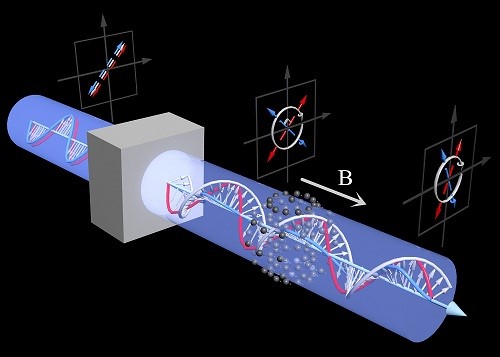
图:单束多色多偏振光法拉第旋光效应原子磁强计方案原理